RF · Signal Processing · FPGA
Spec-to-Hardware: an AI-Orchestrated RF Receiver
A single written specification driving three coupled deliverables — the RF front-end hardware, the signal-processing algorithm model, and the FPGA firmware — demonstrated on a 6-channel frequency-hopping CPFSK receiver. An AI agent drives a trusted deterministic toolchain (MATLAB, RF Toolbox, Simulink, HDL Coder, ModelSim/Vivado) to design, implement, and validate all three, collapsing a years-long, many-handoff process into weeks with an expert in the loop at every stage.
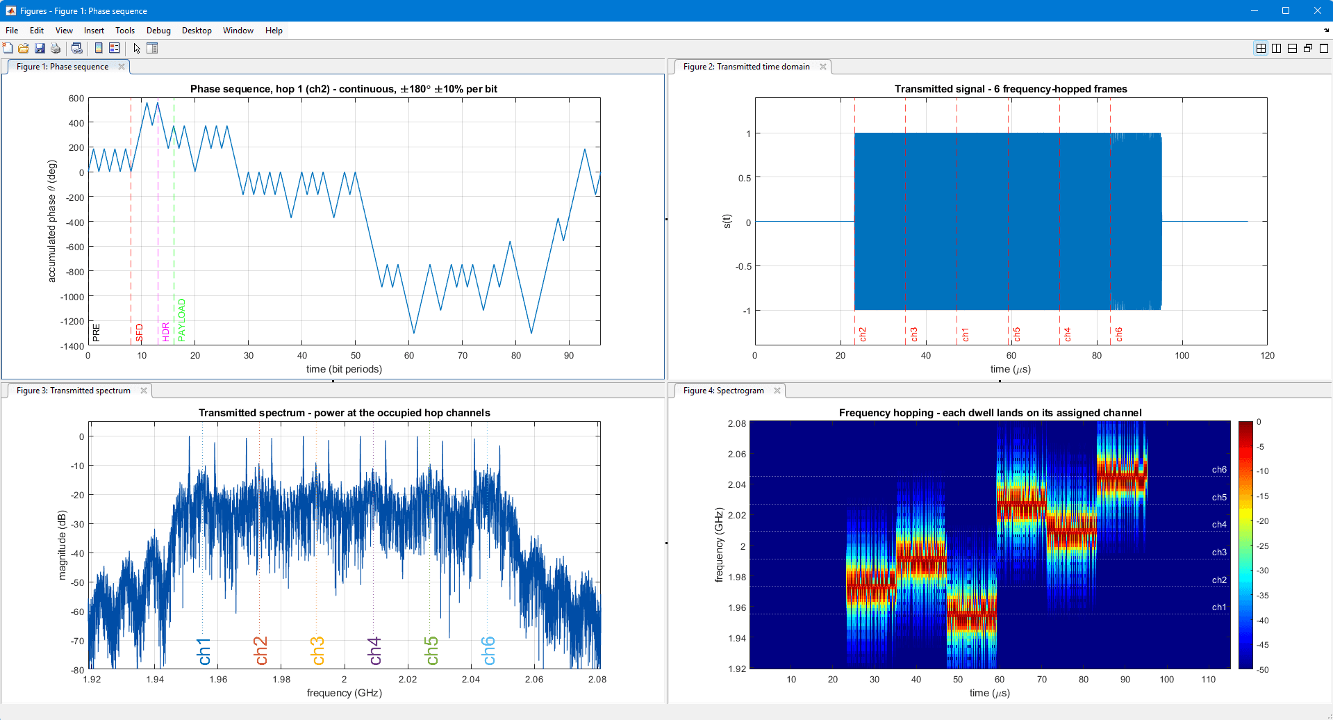
The transmitted signal
A 6-channel FH-CPFSK burst. Each transmission is six dwells; within a dwell the transmitter sends one 96-symbol framed packet — an 8-bit 1010 preamble, a 5-bit SFD, a 3-bit sequence number, an 8-byte payload, and a CRC-16. The receiver must recover every frame under barrage jamming and ±5% symbol-timing variation simultaneously.
Architecture
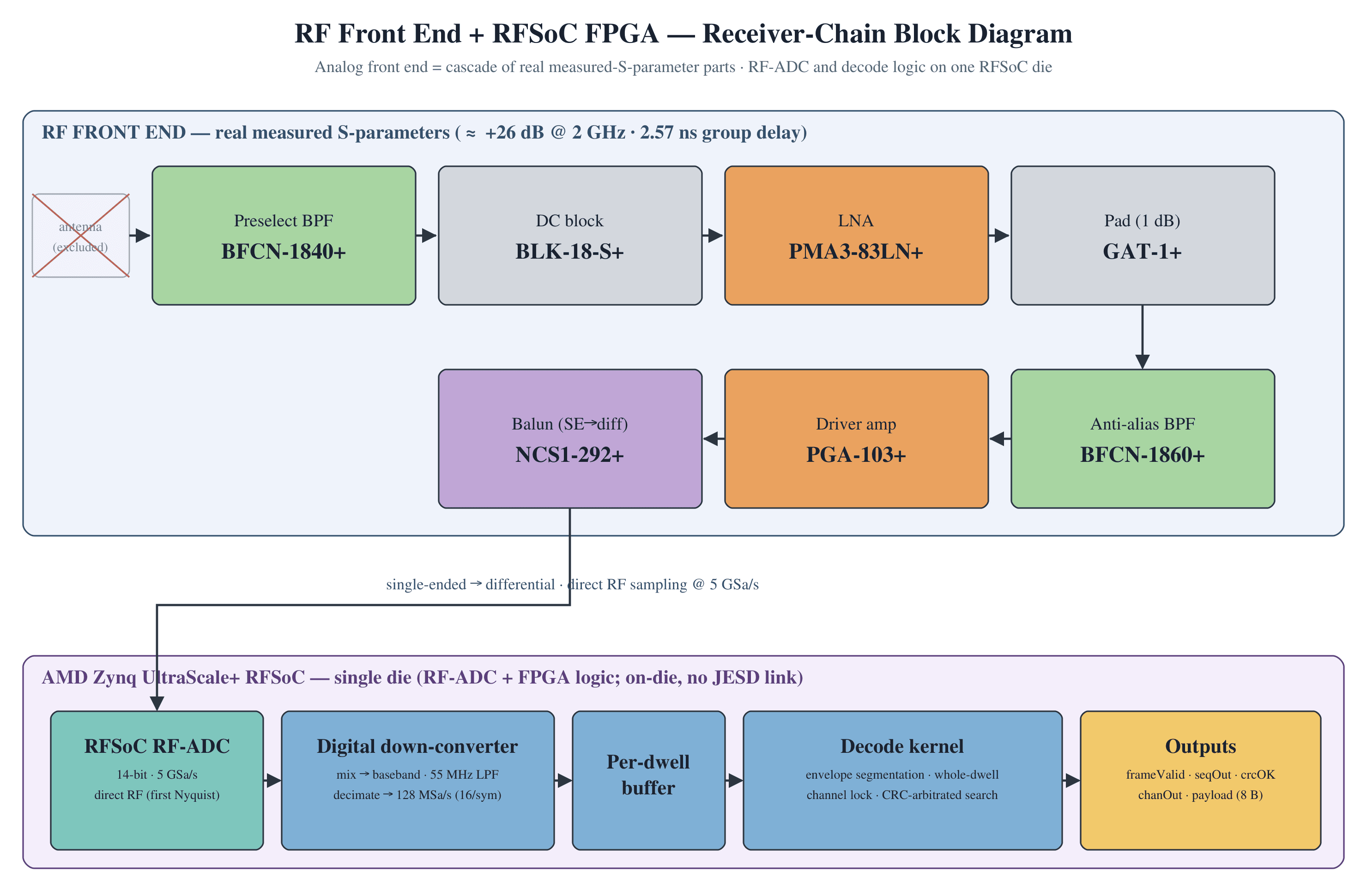
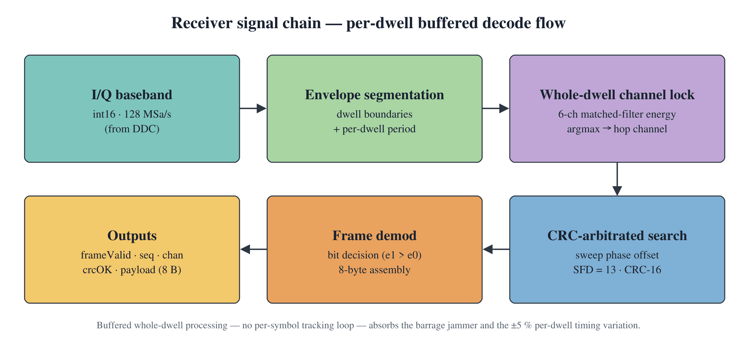
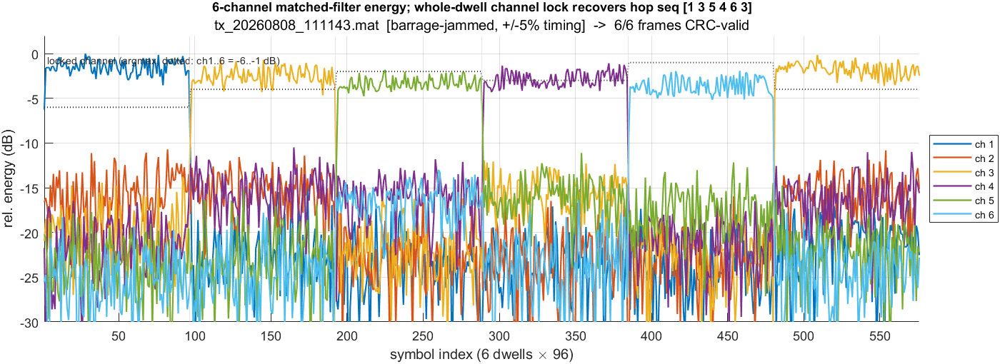
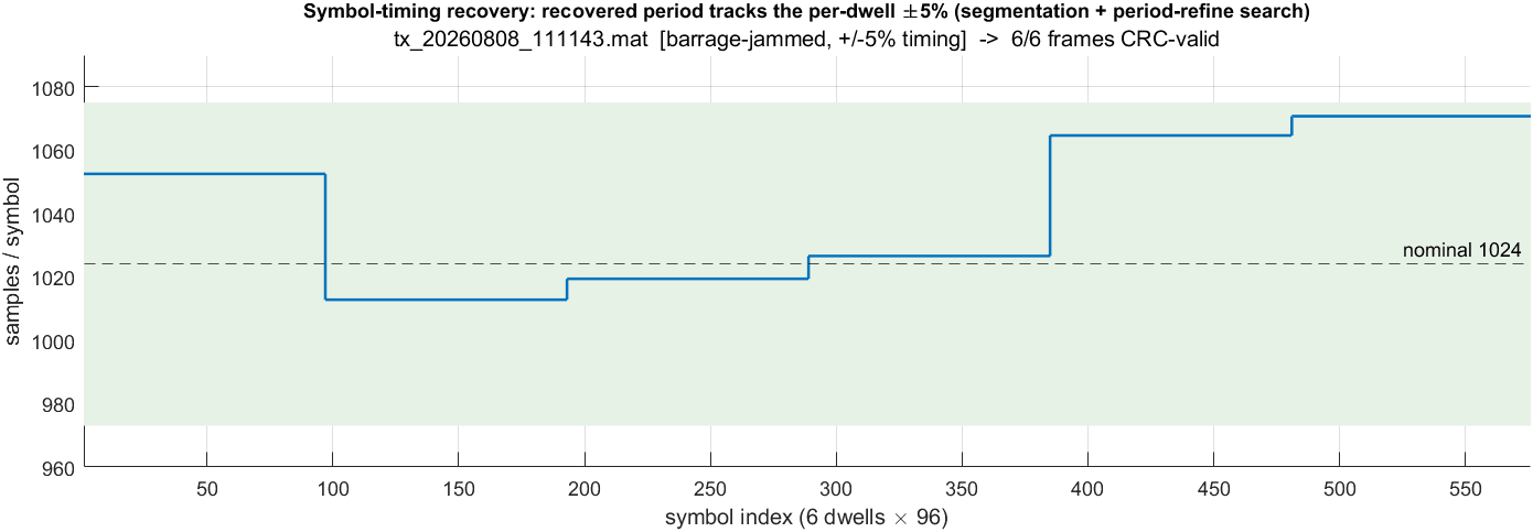
The analog front end is built from the measured S-parameters of real, catalogue commercial parts — an 8-stage cascade feeding a 5 GSa/s RF-ADC. On the RFSoC FPGA, a digital down-converter mixes to complex baseband, low-passes, and decimates to 128 MSa/s. The decode kernel buffers one dwell at a time, measures that dwell's symbol period from its envelope, locks the hop channel, and lets the CRC arbitrate a short phase-offset search for the frame start — a two-pass approach that makes the chain robust to the jammer and the timing variation.
At a glance
| Modulation | Binary continuous-phase FSK (CPFSK) |
| Hopping | 6 channels, 18 MHz spacing, 2.0 GHz center |
| Occupied band | 1.58–2.20 GHz |
| Symbol / bit rate | 8 Msym/s (8 Mbit/s) |
| Converter | 14-bit RFSoC Gen3 RF-ADC, direct sampling @ 5 GSa/s |
| RF front end | 8-stage measured-S-parameter cascade (≈26 dB @ 2 GHz) |
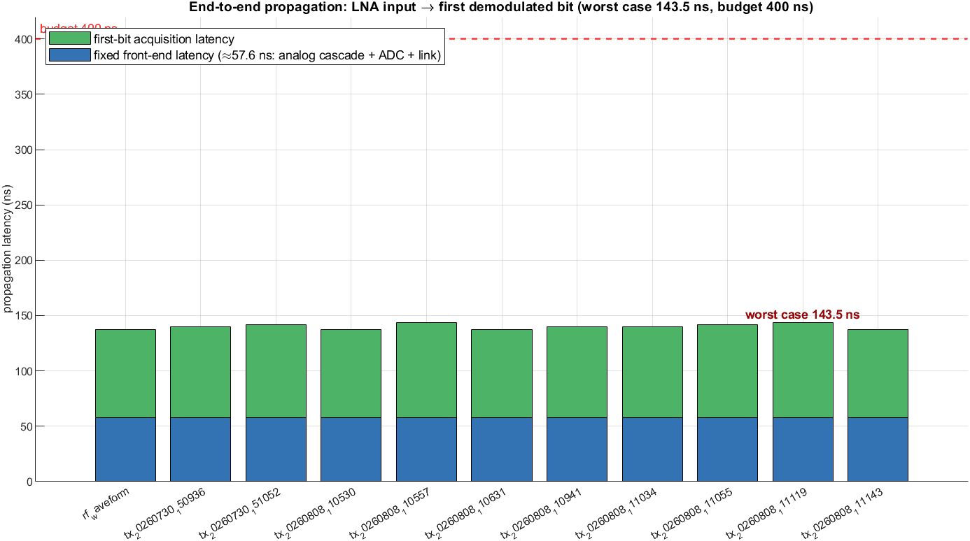
| Latency budget | ≤ 400 ns (worst case achieved: 143.5 ns) |
| Implementation | Fixed-point RTL, HDL-Coder synthesizable |
Real measured RF front end
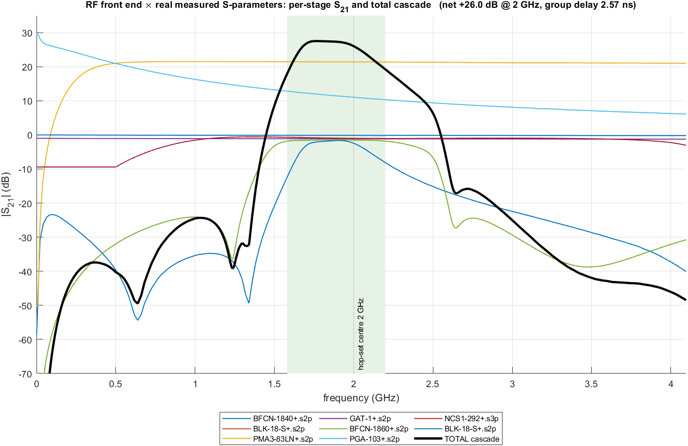
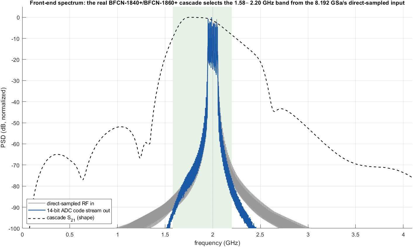
Not an idealized model: each stage is a real catalogue part, applied from its measured Touchstone S-parameters. The BFCN band-pass pair selects the 1.58–2.20 GHz band at ≈ +26 dB with deep out-of-band rejection, and the group delay used in the latency budget is read from the measured phase, not assumed.
The decode kernel, dwell by dwell
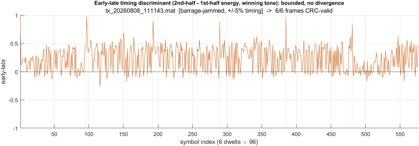
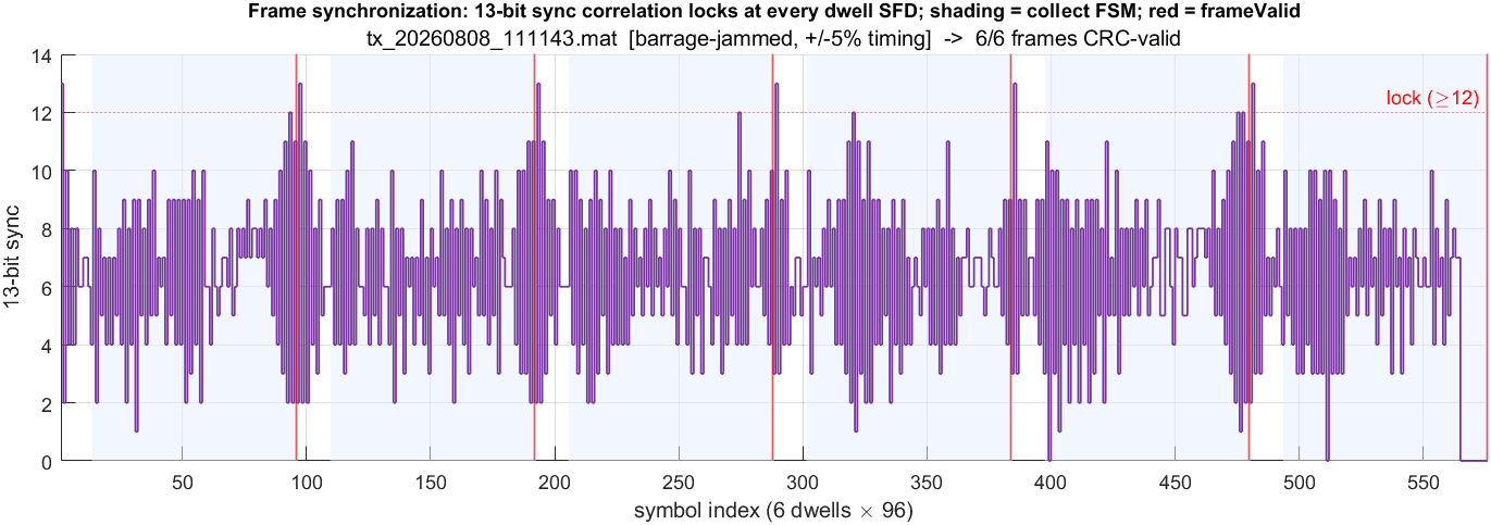
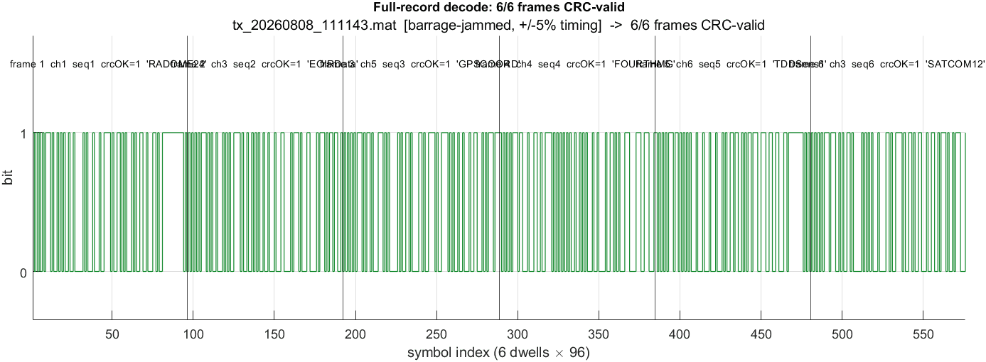
Worked through one barrage-jammed transmission (tx_20260808_111143): the kernel locks each hop channel, recovers the drifting symbol period, confirms per-symbol timing, syncs on the SFD, and decodes all six frames CRC-valid.
Fixed-point core & HDL
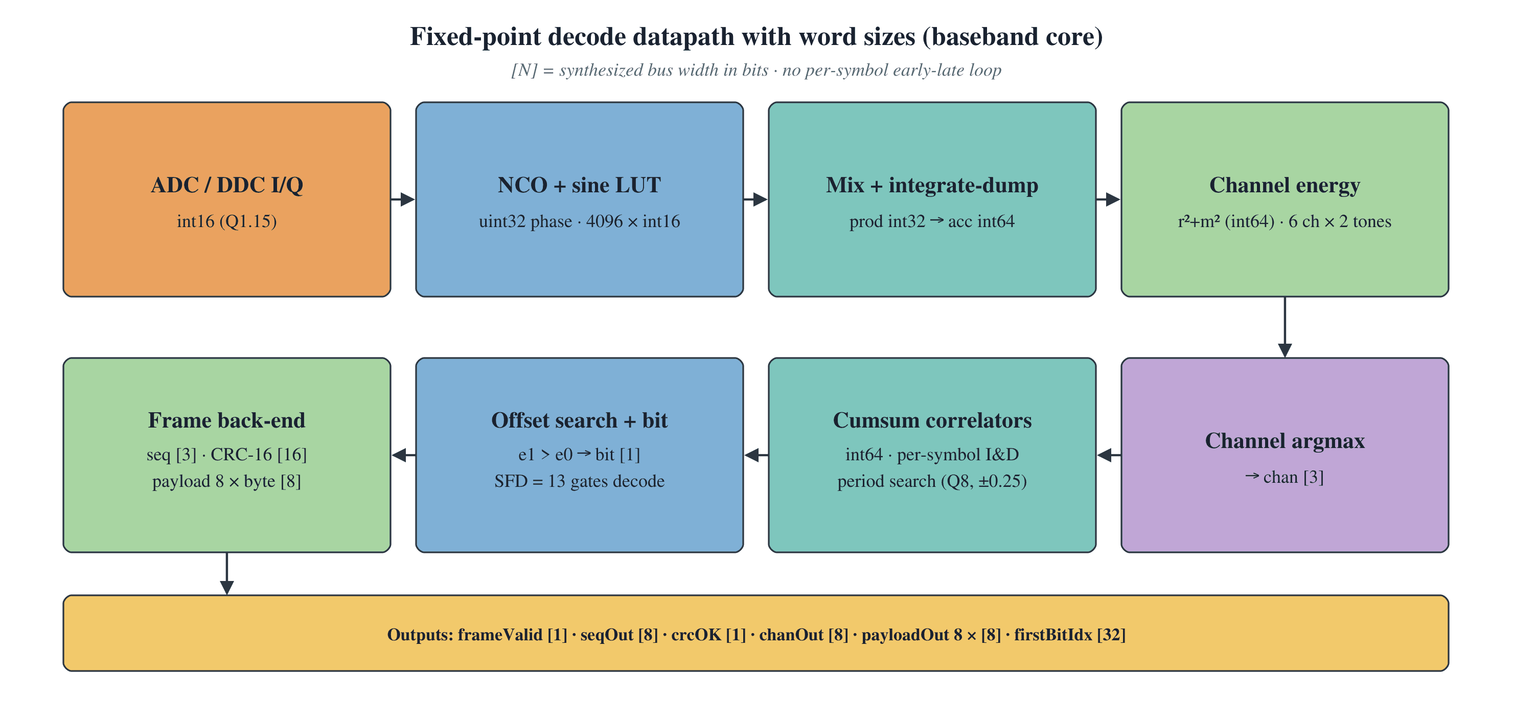
The floating-point reference is converted to a fixed-point datapath and handed to HDL Coder. The generated Verilog is bit-exact against the reference across the whole record.
Results
Every waveform decodes all six frames CRC-valid through the full chain — 3 clean and 8 barrage-jammed / ±5%-timing files, 66/66 frames — with worst-case acquisition latency of 143.5 ns against the 400 ns budget.
| Waveform | Jammed | Frames CRC-valid | Latency (ns) |
|---|---|---|---|
| rf_waveform.mat | No | 6 / 6 | 137.6 |
| tx_20260730_150936.mat | No | 6 / 6 | 139.6 |
| tx_20260730_151052.mat | No | 6 / 6 | 141.6 |
| tx_20260808_110530.mat | Yes | 6 / 6 | 137.6 |
| tx_20260808_110557.mat | Yes | 6 / 6 | 143.5 |
| tx_20260808_110631.mat | Yes | 6 / 6 | 137.6 |
| tx_20260808_110941.mat | Yes | 6 / 6 | 139.6 |
| tx_20260808_111034.mat | Yes | 6 / 6 | 139.6 |
| tx_20260808_111055.mat | Yes | 6 / 6 | 141.6 |
| tx_20260808_111119.mat | Yes | 6 / 6 | 143.5 |
| tx_20260808_111143.mat | Yes | 6 / 6 | 137.6 |
ModelSim verification — live session
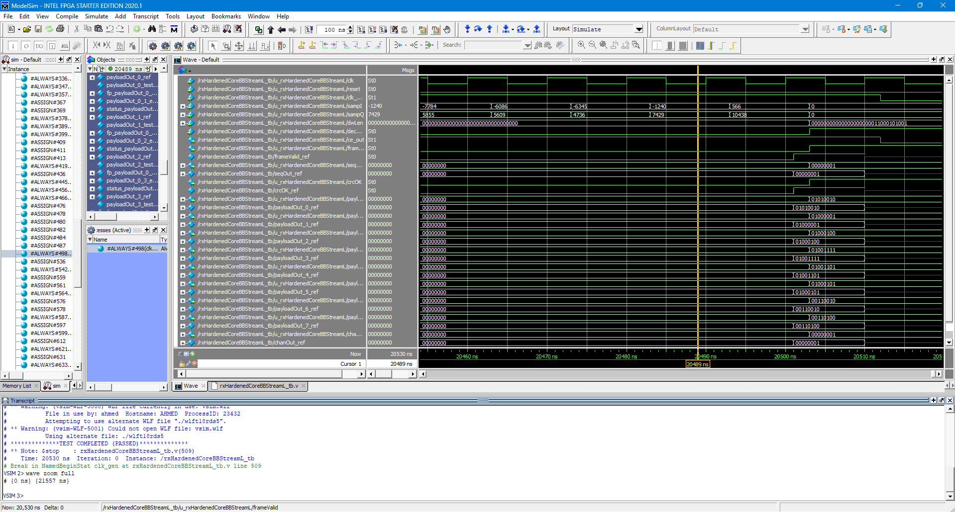
The generated Verilog was simulated live in ModelSim on one barrage-jammed dwell. The self-checking testbench streams the I/Q samples and compares every DUT output against the MATLAB reference sample-by-sample — zero mismatches, with the payload resolving to "RADOME24".
Read the full write-up
The complete technical report and the source code cover the specification, front end, digital down-converter, decode kernel, fixed-point core, HDL, and the live ModelSim verification session.